Morphology of laser-induced damage
Laser-induced damage morphology is a good indicator of the nature linked to damage initiation mechanism.
It can give rough idea about the limiting factor of optical resistance that should be overcome in order to apply optics for high power applications.
Typical examples of various laser induced damage morphologies are listed below:

Pin-points
„Pin-point “ type of defect-driven damage morphology is observed for transparent dielectrics having absorbing inclusions (nanometer sized metallic or dielectric particles) within coatings or uncoated polished surfaces when exposed with nanosecond laser pulses. Pinpoint defects are also observed in bulk materials (for example KDP and DKDP crystals) under different irradiation wavelengths and fluences. Defects are very small (nanometer sized and therefore invisible for optical microscopy) and are produced during manufacturing (link to defects) process. Almost all parameters substrate manufacturing, finishing and deposition technologies have a significant impact on the laser resistance: especially in UV range.
The particle size is closely related to the processes of laser absorption, thermal diffusivity and thermal expansion closely related effects, etc. Under the same irritation energy, the temperature rise is determined by particle size, which can make different size of film damage pits. There is a certain size of metal particle which cause the highest temperature rise and make the film damage easily. Estimation of defect density and its minimization is possible by performing series of tailored LIDT tests while optimizing technology. Please contact Lidaris for details.

Delamination
„Delamination“ type of laser damage appear on coated surfaces together similar like bubbles and blistering.
In this example fracturing of laser annealed and delaminated coating is observed due to high internal (thermally induced) stress or strain of the coating and/or substrate. This type of morphology is typical for dielectric protected metallic coatings.

Fractures and radial cracking
Radial cracking and fractures are typically observed for glasses and crystals irradiated in transparency (infrared-vis ) range with multiple nanosecond and sometimes femtosecond pulses. Typically is a result of localized stress increase due to absorbed laser power and low thermal conductivity. After increase in temperature subsequent processes such as strain, plastic deformation, melt front, and fracture under divergent rather than planar load lead to laser damage. Damage morphology is slightly different for entrance and exit surfaces.

Femtosecond melting
Typical result of “femtosecond melting” is a creation of liquid phase and subsequent ablation in dielectric coatings. Femtosecond laser-induced melting and solidification is observed in the small fluence range between the melting and ablation thresholds. Resolidification occurs after melting leading to the formation of an amorphous layer of having thickness of several tens of nanometers. Depending on coating thickness melting can appear either on surface or within bulk of the coating thus leading to different damage morphology even if the threshold remains the same. The typical timescale of the process and lifetime of the liquid phase is in the range of several tens of nanoseconds.
Droplets and surface melting
Typically observed for metallic coatings and long pulses.

Laser induced contamination
Darkening of surface is observed in optical components operating in vacuum having outgassing parts or dust and gas contaminated environment in air. Smoky areas appear on the surface exhibiting increased absorption even in the visual region thus leading so damage of the coating.

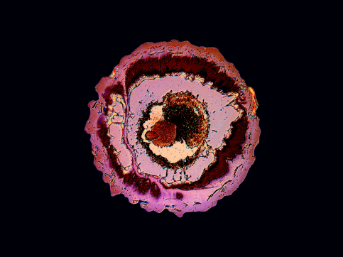
Bulk damage
Laser-induced bulk damage is observed inside transparent materials below entrance surface. Localized heating and annealing effect occurs before the damage and cracking. Exposed sites in crystals also known to exhibit a shell of modified material because of heating and melting under pressure followed by resolidification. This modified material is visible in optical and electron micrographs. The material in the shell often has a different Raman spectrum than undamaged substrate. It is likely that this material is densified, and has a slightly different refractive index than the undamaged material. Bulk fractures may lead to increased scattering and interference effects causing further growth of the damage.

Plasma scalding
defect driven damage is frequently followed by localized melting, boiling, evaporation and plasma formation. High pressure of melted gas result in blurred patterns redeposited o the surface.

Blistering
Laser induced blister or bubble formation is observed in some oxide films after irradiation with either single of multiple femtosecond or nanosecond laser pulses. The shape and dimensions of the blisters vary with the film thickness and incident laser energy. The mechanism responsible for the formation of the blister is thought to be a combination of compressive stress relaxation and the forced expansion of the softened film by material ablated from the substrate. Applications of blister formation include capillaries and channels for micro- and nanofluidics as well as various selective laser ablation/etching of semiconductors for electronics and contact formation.
related Terms and articles
-
 Effective laser pulse widthThe effective pulse width is used to describe laser pulses featuring not rectangular (in example Gaussian or another irregular) shape in time.
 -
 Laser irradiation levelUnits of laser-induced damage threshold
 -
 Morphology of laser-induced damageTypical examples of various laser induced damage morphologies.


